Past reports have focused on the high-level system design, as well as the design, implementation, and validation of the system's various subcells. In this final paper, we present the results of our the integration of these subcells into a working circuit. Simulation results in both IRSIM and HSPICE are presented. Changes since the last report are discussed, as well as the design decisions and optimizations used throughout the design process. Finally, possible future enhancements to the circuit are discussed.
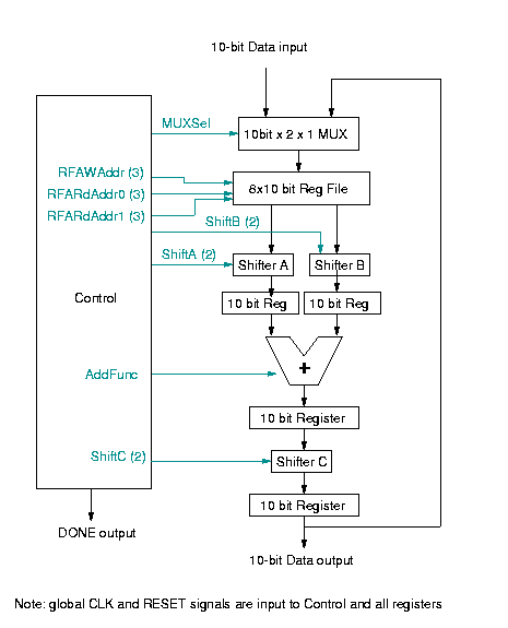
Little has changed in the design of the chip since the last report. The only major differences to the block diagram are the inclusion of the DONE signal, and the elimination of the RFALoad signal. Since the register file loads a new value on every clock cycle, this write enable signal was not necessary. Figure 1 shows the updated block diagram. There were also a few corrections to the microcode since the last report. The new microcode is shown in Appendix A of this report.
The main challenge of integration was finding a geometric layout of the subcells that would create a compact chip. Unfortunately not all of the subcells are of the same size and shape, so this was a nontrivial task. The resulting layout is reasonably dense, although there is some wasted area. The layout could be tweaked to further reduce its area. However, if area were a major concern in the end application, probably taking another approach to the circuit's design, such as using dynamic logic, would be more beneficial than tweaking the current design to save a few square microns.
The integration process was fairly straightforward. In some places we had to add buffers or inverters so that the subcells could communicate correctly. For example, the outputs of the ROM have a limited voltage swing. Static buffers were therefore inserted on the outputs of the ROM to improve noise margins.
A non-obvious problem with our adder/subtractor was discovered during the integration process. When the adder/subtractor was simulated as an independent unit, it performed perfectly. However when integrated into the circuit, it output undefined values during subtraction operations. Upon investigation, we discovered a fan-in problem with the pass transistor XOR gates used in the adder/subtractor. A single inverter had been used to drive the inputs of all 10 XOR gates. We discovered that the single inverter could not drive all of these gates successfully. The problem had not been discovered during simulation of the adder/subtractor itself because inputs into IRSIM and HSPICE are ideal voltage sources (zero output impedance). The problem was solved by adding more inverters such that only two XOR gate inputs are driven by a single inverter.
The inputs for the chip are:
The chip's outputs are:
The chip's subcells have been discussed in detail in previous reports, and remain unchanged. Table 1 summarizes some of the characteristics of the subcells.
| Adder/Subtractor | Static ripple-carry mirror adder | 3.88ns | 1863 sq micron |
| Shifter | Pass transistors | 0.95 ns | 1195 sq micron |
| Control | Static register and incrementer; pseudo-NMOS NOR ROM and decoder | 0.68 ns | 7305 sq micron |
| Register File | Static decoder; array of static D flip-flops | 2.76 ns | 34910 sq micron |
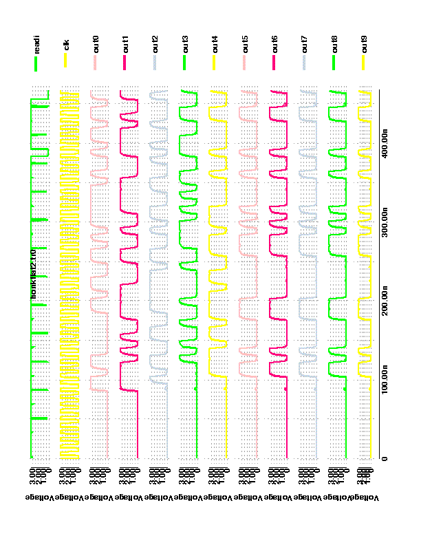
We discuss the simulation of the chip in detail in Section IV of this report. Table 2 summarizes some of the chip characteristics determined by the HSPICE simulation for a single 8-item IDCT transform.
| Total area | 212.8 x 339.0 = 72139 sq micron |
| Total time | 550 ns |
| Average power | 9.6626E-2 |
| Maximum power | 2.5299E-1 |
| Minimum clock period | 8.0 ns |
Debugging using IRSIM proceeded as follows. IRSIM command files with sample DCT coefficients were developed, and IRSIM was run on them. Appendix B contains an example of an IRSIM command file. The results were checked using a C program which performed the same arithmetic as the circuit (based on the program presented in the Project Interim report). This allowed errors in the circuit (mostly in the ROM microcode) to be found and corrected.
We also wished to verify that the circuit would work in an actual application. This would verify both the correctness of the circuit's computations as well as correct interaction with an external device. To do this, the code for the Berkeley mpeg_play decoder was modified. We replaced the IDCT routine in mpeg_play with code that generated an appropriate IRSIM command file, executed IRSIM on this command file, and parsed the results. We then ran mpeg_play on a sample MPEG video file. The modified mpeg_play source is available at http://www.cse.psu.edu/~crandall/cse477/report4/code/. The modifications were made to the floatdct.c and video.c source files.
This simulation was a herculean task. This 320x240 image required some 19,200 IDCT calculations. In other words, IRSIM had to be run nearly twenty thousand times. Unfortunately an IRSIM simulation of the the IDCT unit takes roughly 100 million times the amount of time that the actual circuit would take! This simulation for decoding a single frame therefore required about 36 hours of CPU time on a very fast 300-MHz Silicon Graphics Octane workstation.
However, the reward of this time-consuming simulation is very compelling evidence that the circuit works well. Figure 4 shows the results of an MPEG frame decode using our IDCT unit at the core. The quality of the decoded frame is good, despite the approximations made in our algorithm.

HSPICE simulation was also time-consuming. Simulation of the above-mentioned circuit required about 2 hours of processing time and generated a 400 megabyte output file. A workstation with a gigabyte of physical RAM was necessary to view this output file, since on other machines, NST crashed (probably due to running out of memory).
The results of the simulation were presented previously in Table 2. The maximum power occurred during clock cycle 44, but this seems to depend on the values DCT coefficients being transformed.
The HSPICE simulation results were also used to determine the critical paths in our data path. The two worst-case delays were the adder with 5.23 ns, and the register file with 4.18 ns. Along with the setup time and propagation delay of the pipeline registers, propagation delay of the control unit, and finite rise and fall time of the clock (set to 0.5 ns each in this simulation), this would imply a minimum clock period of about 8.0 ns.
For example, initially a multiplier was envisioned for the unit to compute the exact IDCT. However designing and incorporating a multiplier in the circuit would have been intractable for this project. Instead, the multiplier was replaced by a shifter, and products were approximated to powers of two.
Also, all subcells were built and tested separately and then integrated together as the last step. This allowed subcells to be reused in the project and also aided in ease of debugging. If design time had not been a concern, the entire data path would have been designed at once in a bit-sliced fashion, resulting in a more compact design.
Another example is found in the adder/subtractor subcell of our circuit. We chose a simple ripple-carry adder because of ease of implementation. If we had been optimizing for speed, we might have chosen a more efficient adder circuit. However since for small numbers of bits the ripple-carry adder performs nearly as well (or better) than the other types of adders, we decided that it was a reasonable implementation for our circuit.
Note that we are not using this as an excuse to be lazy. To the contrary, in many cases we have carefully optimized for speed, area, and power. However, when reasonable, we have chosen easier design options so that time could be spent on other, more interesting parts of the design.
Since the circuit is a pipeline, only the critical subcells are worth considering for speed optimization. In our case, this would be the adder subcell, the control unit, and the registers. The registers were improved simply by removing features from our D flip-flop which are not necessary for these registers. For example, the load and output enable features were removed, since the registers in the datapath always load and always output on every clock cycle.
Probably the most significant improvement to speed was accomplished by switching to a pipeline design, as discussed in the Project Prototype Report. The original design required nearly 80 states and did not use a pipeline approach, so both the number of states and the minimum clock period was greater. The new design requires only 49 states and the pipeline allows for a faster clock period.
Area optimizations were made at the gate level as well. Pass-transistor logic was used to compactly implement devices such as multiplexers and XOR gates.
In some instances, area savings were accomplished by not reusing components built for other parts of the circuit. For example, it was tempting to use our adder circuit to generate the address in the control unit. But the control unit always advances through the ROM addresses one at a time. Therefore the adder was simplified to an increment circuit and consumed a much smaller area.
We noticed that one major source of wasted power are the glitches on the control signals caused by the ROM. Unfortunately the PMOS transistors in the ROM pull the outputs high briefly when an output is 0 in two successive clock cycles. This causes many of the transistors in the circuit to switch unnecessarily.
We discuss in Section VI some of the ways this could be corrected. However we noticed a simple way to reduce this problem. There are many (about 10%) of the bits in the ROM that are don't-cares. Initially these were coded as 0's. However we later changed these to 1's, since this alleviated the 0 to 0 glitch problem. This minor change reduced the power consumed by the circuit by about 15%.
One of the strong points of the circuit is its modularity and simplicity. It achieves a reasonably accurate approximation of the IDCT without a multiplier, and this makes it small and fast. However if in the future more accurate computations were necessary, a multiplier could be incorporated into the system with minimal changes. Most of the subcells could be reused, and the ROM could be easily programmed with the new microcode.
It was shown previously in this report that a minimum clock speed of about 9ns would be required for this IDCT unit to be useful in decoding 640x480 MPEG videos in real-time. Our clock speed of 8ns fits within this constraint.
However there is always room for improvement. One possible way to improve the circuit would be to redesign it using a dynamic approach. This would significantly reduce the area and delay of the circuit. The datapath could be redesigned using DOMINO logic or NORA. Since all registers in the register file are written to often, an explicit refresh would probably not even be required for the register file.
As mentioned earlier, the area of the circuit could probably be reduced a little using a more compact integration of the subcells. However the current design is relatively dense.
Unfortunately the circuit exhibits a number of glitches. Although they do not affect functionality, they do cause wasted power due to unnecessary transistor switches. As mentioned early, a glitch can occur between adjacent 0's in the output signals. The static subcells respond to the glitches by switching accordingly. We made some attempts to reduce this using intelligent values for don't cares, but the problem still exists. One possible solution to this problem would be to switch to a dynamic approach for the ROM and decoder arrays and disconnect the outputs of the ROM during the precharge phase. The ROM and decoder arrays themselves would save power this way, too, since pseudo-NMOS logic consumes more power than dynamic logic (due to the direct path from VDD to ground).
Although an effort was made to size transistors appropriately, some hazards do appear within the subcells as well. For example, in the shifter, a glitch occurs when the function inputs change from 11 to 00. This is caused by unequal propagation delays to two inputs of a NAND gate. Equalizing the delay would fix this problem.
Since the slowest unit in the pipeline is the adder, efforts to improve the speed of the circuit should be focused there. Possible approaches would be to use a more sophisticated adder design, such as one of the look-ahead adders.
I enjoyed this project, although it was very time-consuming and frustrating at times. However the amount that I learned from the project justified the time requirements. Only after implementing circuits on my own have I started to understand some of the concepts presented in class. For example, without struggling to layout complex circuits, I would not have learned as much about issues in designing adders, shifters, ROMs, etc.
M R R R R S S S A R
U F F F F A B C D E
X A A A A D A
S L W R R M D
E D A A A D Y
L 0 1

#### load data from input (8 cycles)
0 1 001 xxx xxx xx xx xx x 0
0 1 010 xxx xxx xx xx xx x 0
0 1 100 xxx xxx xx xx xx x 0
0 1 110 xxx xxx xx xx xx x 0
0 1 000 xxx xxx xx xx xx x 0
0 1 111 000 000 00 11 xx x 0 # R0a <- Rf0, R0b <- Rf0/2
0 1 101 001 001 00 11 xx 0 0 # R0a <- Rf1, R0b <- Rf1/2, R1 <- R0a+R0b

0 1 011 101 100 00 11 11 0 0 # s2[3] # R2 <- R1/2, R1 <- R0a+R0b, R0a <- Rf5, R0b <- Rf4/2
1 1 000 011 010 10 11 11 1 0 # s2[6] # Rf0 <- R2, R2 <- R1/2, R1 <- R0a-R0b, R0a <- Rf3*2, R0b <- Rf2/2
1 1 001 010 011 10 11 10 1 0 # s2[4] # Rf1 <- R2, R2 <- R1*2, R1 <- R0a-R0b, R0a <- Rf2*2, R0b <- Rf3/2
1 1 011 110 111 00 11 00 0 0 # s2[5] # Rf3 <- R2, R2 <- R1, R1 <- R0a+R0b, R0a <- Rf6, R0b <- Rf7
1 1 110 111 110 00 11 00 0 0 # s2[7] # Rf6 <- R2, R2 <- R1, R1 <- R0a+R0b, R0a <- Rf7, R0b <- Rf6
1 1 100 100 101 00 11 10 1 0 # s2[1] # Rf4 <- R2, R2 <- R1*2, R1 <- R0a-R0b, R0a <- Rf4, R0a <- Rf5/2
1 1 101 000 001 00 00 10 0 0 # s2[0] # Rf5 <- R2, R2 <- R1*2, R1 <- R0a+R0b, R0a <- Rf0, R0b <- Rf1
1 1 111 001 000 00 00 10 0 0 # s2[2] # Rf7 <- R2, R2 <- R1*2, R1 <- R0a+R0b, R0a <- Rf1, R0b <- Rf0

1 1 001 011 xxx 00 01 10 1 0 # s3[6] # Rf1 <- R2, R2 <- R1*2, R1 <- R0a-R0b, R0a <- Rf3, R0b <- 0
1 1 000 110 111 00 00 10 x 0 # s3[1] # Rf0 <- R2, R2 <- R1*2, R1 <- R0a+R0b, R0a <- Rf6, R0b <- Rf7
1 1 010 110 111 00 00 00 1 0 # s3[7] # Rf2 <- R2, R2 <- R1, R1 <- R0a-R0b, R0a <- Rf6, R0b <- Rf7
1 1 110 001 xxx 00 01 11 0 0 # s3[4] # Rf6 <- R2, R2 <- R1/2, R1 <- R0a+R0b, R0a <- Rf1, R0b <- 0
1 1 001 100 101 00 00 11 x 0 # s3[0] # Rf1 <- R2, R2 <- R1/2, R1 <- R0a+R0b, R0a <- Rf4, R0b <- Rf5
1 1 111 100 101 00 00 00 0 0 # s3[3] # Rf7 <- R2, R2 <- R1, R1 <- R0a+R0b, R0a <- Rf4, R0b <- Rf5
1 1 100 000 xxx 00 01 11 1 0 # s3[2] # Rf2 <- R2, R2 <- R1/2, R1 <- R0a-R0b, R0a <- Rf0, R0b <- 0
1 1 000 010 xxx 00 01 11 x 0 # s3[5] # Rf0 <- R2, R2 <- R1/2, R1 <- R0a+R0b, R0a <- Rf2, R0b <- 0

1 1 011 000 xxx 00 01 00 x 0 # s5[1] # Rf3 <- R2, R2 <- R1, R1 <- R0a+R0b, R0a <- Rf0, R0b <- 0
1 1 010 001 xxx 00 01 00 x 0 # s5[5] # Rf2 <- R2, R2 <- R1, R1 <- R0a+R0b, R0a <- Rf1, R0b <- 0
1 1 101 110 111 00 00 00 x 0 # s5[3] # Rf5 <- R2, R2 <- R1, R1 <- R0a+R0b, R0a <- Rf6, R0b <- Rf7
1 1 001 101 011 00 00 00 0 0 # s5[6] # Rf1 <- R2, R2 <- R1, R1 <- R0a+R0b, R0a <- Rf5, R0b <- Rf3
1 1 101 101 011 00 00 11 1 0 # s5[2] # Rf5 <- R2, R2 <- R1/2, R1 <- R0a-R0b, R0a <- Rf5, R0b <- Rf3
1 1 011 110 111 00 00 11 0 0 # s5[7] # Rf3 <- R2, R2 <- R1/2, R1 <- R0a+R0b, R0a <- Rf6, R0b <- Rf7
1 1 110 010 100 00 00 11 1 0 # s5[0] # Rf6 <- R2, R2 <- R1/2, R1 <- R0a-R0b, R0a <- Rf2, R0b <- Rf4
1 1 010 010 100 00 00 11 0 0 # s5[4] # Rf2 <- R2, R2 <- R1/2, R1 <- R0a+R0b, R0a <- Rf2, R0b <- Rf4

1 1 111 010 011 00 00 11 1 0 # s6[2] # Rf7 <- R2, R2 <- R1/2, R1 <- R0a-R0b, R0a <- Rf2, R0b <- Rf3
1 1 000 010 011 00 00 11 0 0 # s6[1] # Rf0 <- R2, R2 <- R1/2, R1 <- R0a+R0b, R0a <- Rf2, R0b <- Rf3
1 1 100 000 001 00 00 11 1 0 # s6[7] # Rf4 <- R2, R2 <- R1/2, R1 <- R0a-R0b, R0a <- Rf0, R0b <- Rf1
1 1 010 000 001 00 00 11 1 0 # s6[0] # Rf2 <- R2, R2 <- R1/2, R1 <- R0a-R0b, R0a <- Rf0, R0b <- Rf1
1 1 001 110 111 00 00 11 0 0 # s6[5] # Rf1 <- R2, R2 <- R1/2, R1 <- R0a+R0b, R0a <- Rf6, R0b <- Rf7
1 1 111 110 111 00 00 11 0 0 # s6[6] # Rf7 <- R2, R2 <- R1/2, R1 <- R0a+R0b, R0a <- Rf6, R0b <- Rf7
1 1 000 100 101 00 00 11 1 0 # s6[3] # Rf0 <- R2, R2 <- R1/2, R1 <- R0a-R0b, R0a <- Rf4, R0b <- Rf5
1 1 101 100 101 00 00 11 1 0 # s6[4] # Rf5 <- R2, R2 <- R1/2, R1 <- R0a-R0b, R0a <- Rf4, R0b <- Rf5

1 1 110 000 xxx 00 01 11 0 0 # # Rf6 <- R2, R2 <- R1/2, R1 <- R0a+R0b, R0a <- Rf0, R0b <- 0
1 1 011 001 xxx 00 01 11 x 0 # # Rf3 <- R2, R2 <- R1/2, R1 <- R0a+R0b, R0a <- Rf1, R0b <- 0
1 1 100 010 xxx 00 01 00 x 1 # # Rf4 <- R2, R2 <- R1, R1 <- R0a+R0b, R0a <- Rf2, R0b <- 0
1 0 000 011 xxx 00 01 00 x 0 # # R2 <- R1, R1 <- R0a+R0b, R0a <- Rf3, R0b <- 0
1 0 000 100 xxx 00 01 00 x 0 # # R2 <- R1, R1 <- R0a+R0b, R0a <- Rf4, R0b <- 0
1 0 000 101 xxx 00 01 00 x 0 # # R2 <- R1, R1 <- R0a+R0b, R0a <- Rf5, R0b <- 0
1 0 000 110 xxx 00 01 00 x 0 # # R2 <- R1, R1 <- R0a+R0b, R0a <- Rf6, R0b <- 0
1 0 000 111 xxx 00 01 00 x 0 # # R2 <- R1, R1 <- R0a+R0b, R0a <- Rf7, R0b <- 0
1 0 000 xxx xxx xx xx 00 x 0 # # R2 <- R1, R1 <- R0a+R0b
1 0 000 xxx xxx xx xx 00 x 0 # # R2 <- R1
display -automatic
vector in in9 in8 in7 in6 in5 in4 in3 in2 in1 in0
vector muxout d9 d8 d7 d6 d5 d4 d3 d2 d1 d0
vector rfaout qa9 qa8 qa7 qa6 qa5 qa4 qa3 qa2 qa1 qa0
vector rfbout qb9 qb8 qb7 qb6 qb5 qb4 qb3 qb2 qb1 qb0
vector out out9 out8 out7 out6 out5 out4 out3 out2 out1 out0
vector controlout o0 o1 o2 o3 o4 o5 o6 o7 o8 o9 o10 o11 o12 o13 o14 o15 o16
vector rax ra2 ra1 ra0
vector rbx rb2 rb1 rb0
vector wx w2 w1 w0
vector addo addo9 addo8 addo7 addo6 addo5 addo4 addo3 addo2 addo1 addo0
vector sha sha9 sha8 sha7 sha6 sha5 sha4 sha3 sha2 sha1 sha0
vector shb shb9 shb8 shb7 shb6 shb5 shb4 shb3 shb2 shb1 shb0
vector shc shc9 shc8 shc7 shc6 shc5 shc4 shc3 shc2 shc1 shc0

unitdelay 10
w in muxout rfaout rfbout out controlout
w clk reset
w sha shb shc addo rax rbx wx
w func funcnot
w ready

stepsize 100000
clock clk 0 1
l reset
c
c

h reset
s 1000

set in 0000000001
c
set in 0000111111
c
set in 0010000100
c
set in 0000100001
c
set in 0000000000
c
set in 0000000000
c
set in 1111101010
c
set in 0000000000
c

c 34
d out
c
d out
c
d out
c
d out
c
d out
c
d out
c
d out
c
s 100000
d out
exit
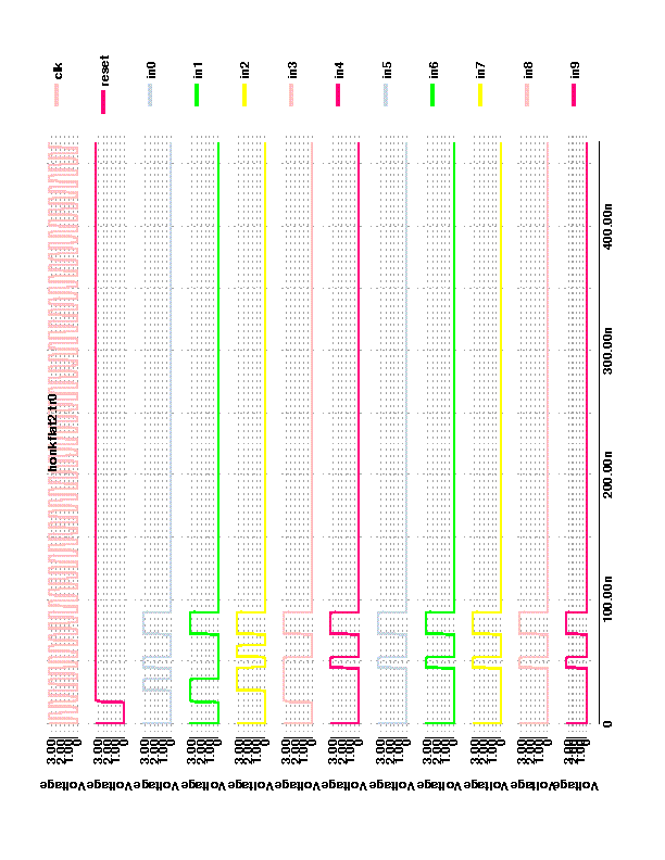
VDD 3.3
CLK 5.5
RISE 0.5
FALL 0.5
clk 010101010101010101010101010101010101010101010101010101010101010101010101010101010101010101010101010101
in9 000000000011000011110000000000000000000000000000000000000000000000000000000000000000000000000000000000
in8 000000000011000011110000000000000000000000000000000000000000000000000000000000000000000000000000000000
in7 000000000011000011110000000000000000000000000000000000000000000000000000000000000000000000000000000000
in6 000000000011000011110000000000000000000000000000000000000000000000000000000000000000000000000000000000
in5 000000000011000011110000000000000000000000000000000000000000000000000000000000000000000000000000000000
in4 000000000011000011110000000000000000000000000000000000000000000000000000000000000000000000000000000000
in3 000011111111000011110000000000000000000000000000000000000000000000000000000000000000000000000000000000
in2 000000111100110011110000000000000000000000000000000000000000000000000000000000000000000000000000000000
in1 000011110000000011110000000000000000000000000000000000000000000000000000000000000000000000000000000000
in0 000000110011000011110000000000000000000000000000000000000000000000000000000000000000000000000000000000
reset 000011111111111111111111111111111111111111111111111111111111111111111111111111111111111111111111111111